Description
The module is designed for both Industrial and commercial applications. The latest device technologies and design methods are employed to offer high power density, efficiency, and linearity in a small, lightweight package.
Specification
Typical performance at +28V DC +25oC, and in a 50Ω system.
RF / ELECTRICAL | ||||
PARAMETER | MIN | TYP. | MAX | UNIT |
Operating Frequency | 12.9 | 13.1 | GHz | |
RF INPUT | 0 | dBm | ||
Power Gain | 49 | dB | ||
P-1dB Output Power | 49 | dBm | ||
Power Gain temperature drift | 3 | dB | ||
In/Out Impedance | 50 | Ω | ||
Input VSWR | 1.3 | |||
Spurious Signals | -55 | dBc | ||
IMD3@Output 42dbm @ two tone space 5MHz | -25 | dBc | ||
Operating Voltage | 28 | V DC | ||
Power Dissipation | 700 | W | ||
MECHANICAL | ||
PARAMETER | VALUE | UNIT |
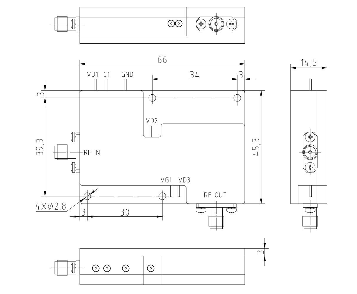
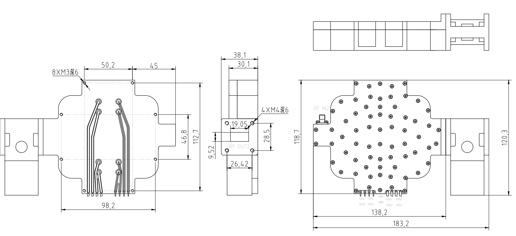
Dimensions (W x D x H) | 66*45.3*12 mm (SW-DRIPA-1290013100-31C) 183.2*120.3*38.1mm(SW-FINPA-1290013100-49C) | mm |
RF Connectors (Input / Output) | SMA-KF / WR75 (Flange BJ120) | — |
Control Connector | Radio frequency powered insulator | — |
Cooling | Forced air cooling for heat dissipation( A radiator needs to be installed.) | — |
Weight | ≤8 | kg |
ENVIRONMENTAL / PROTECTIONS | |||
PARAMETER | MIN | MAX | UNIT |
Operating Temp. | 0 | +55 | °C |
Humidity Range | 0-100 | % | |
Amplifier Safeguard Temp. | +80 | °C | |
Protections | Output mismatch protection | ||
INPUT/OUTPUT panel Connector | |||
AMPLIFIER CONNECTOR TYPE: | —— | ||
TRIAD CABLE PART NUMBER: | —— | ||
NUMBER | interface type | DESCRIPTION | |
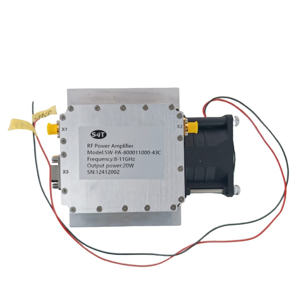
X1 | SMA-FK | RF IN1 | |
X2 | SMA-FK | RFOUT1 | |
X3 | SMA-FK | RFIN2 | |
X4 | WR75 | RFOUT2 | |
Connector Definition | ||
AMPLIFIER CONNECTOR TYPE: | ||
TRIAD CABLE PART NUMBER: | —— | |
NUMBER | Definition | DESCRIPTION |
Drive amplifica Drive amplification module (SW-DRIPA-1290013100-31C) | ||
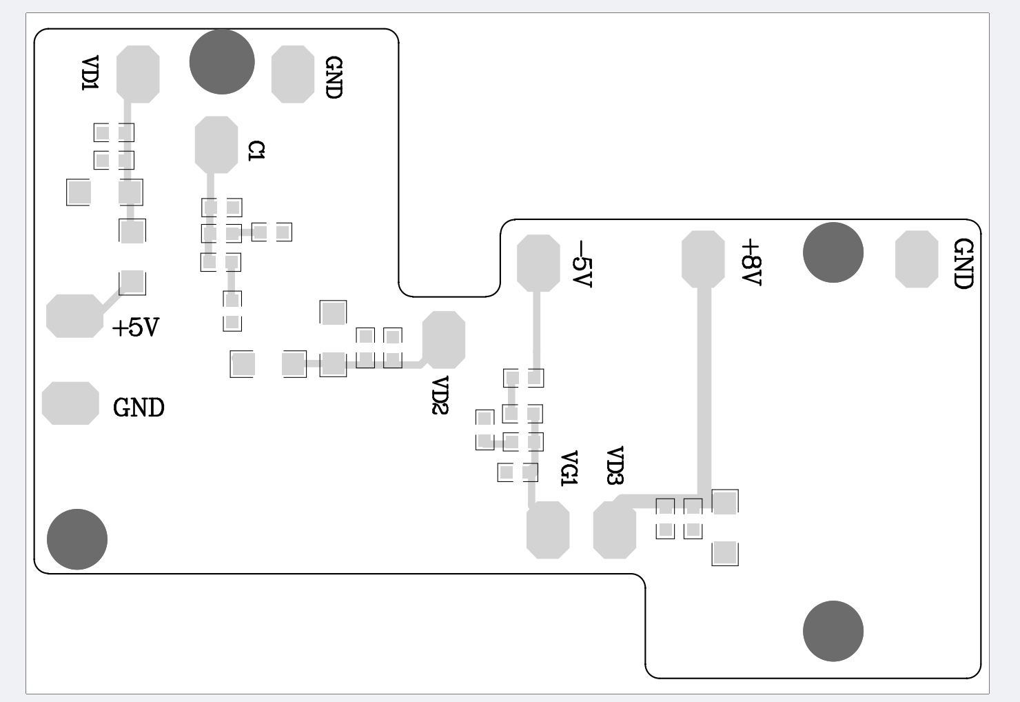
1 | VD1 | +3.5V (≤200mA) |
2 | C1 | +1.05V(≤100mA) |
3 | GND | GND |
4 | VD2 | +3.5V (≤200mA) |
5 | VG1 | -1V(≤100mA) |
6 | VD3 | +8V(≤1.8A) |
Final amplification module(SW-FINPA-1290013100-49C) | ||
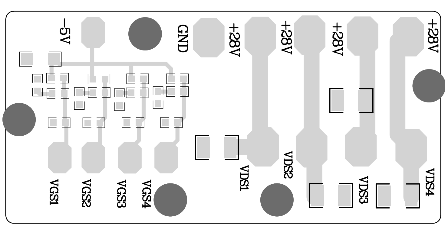
7 | VGS1 | -1.9V(≤100mA) |
8 | VGS2 | -1.9V(≤100mA) |
9 | VGS3 | -1.9V(≤100mA) |
10 | VGS4 | -1.9V(≤100mA) |
12 | VDS1 | +28V(≤6A) |
13 | VDS2 | +28V(≤6A) |
14 | VDS3 | +28V(≤6A) |
15 | VDS4 | +28V(≤6A) |
16 | GND | GND |
Drive amplification module (SW-DRIPA-1290013100-31C)
Cover plate installation PCB (SW-DRIPA-1290013100-31C)
Final amplification module(SW-FINPA-1290013100-49C)
Cover plate installation PCB (SW-FINPA-1290013100-49C)